Quantcast
Channel: Data converters forum - Recent Threads
Viewing all 5988 articles
Browse latest View live

ADC12DJ3200: timestamp input common mode and capacitor before balun

$
0
0

Part Number:ADC12DJ3200

Hi TI,

We are using ADC12DJ3200 in our project.

ADC12DJ3200 will be interfaced with virtex-7 XC7VX485T FPGA.

We have two questions:

1. Common mode voltage for timestamp input in ADC12DJ3200 datasheet is 0.3v typical.

  We will be connecting the timestamp inputs of ADC12DJ3200 to virtex-7 FPGA using LVDS standard in FPGA.

  Now the common mode for LVDS output of FPGA is 1.25v.

  So, do we need to AC couple the timestamp inputs and provide the necessary common mode for timestamp inputs using pull up and pull down resistors on timestamp inputs?

  And if pull up resistors are required , which power supply should we use (1.9v analog, 1.1v analog, 1.1v digital) for pull ups?

2. We are using only balun (BAL-0009SMG) for input signal to ADC inputs. Do we also need to use capacitor between SMA connector and BALUN?

Thanks,

Lalit


ADC34J44EVM: Coherently clocking multiple boards

$
0
0

Part Number:ADC34J44EVM

Hi

 I want to sample 8 channels simultaneously at 125MSPS. If I use two ADC34J44EVM boards for sampling these 8 channels with two TSW14J56EVM boards for data capture, can I make all the 8 channels sample coherently with one computer? 

DAC37J84: SPI state when powered down

$
0
0

Part Number:DAC37J84

When the device is powered down, what's the state of the SPI bus? Does the device pull it low? I have it sharing the bus with other devices. I'd like to turn the device off when not used to conserve power, but will this make the SPI bus not accessible to other devices on the bus? 

DAC7678EVM: Reading output voltages on DAC7678

$
0
0

Part Number:DAC7678EVM

I'm interfacing with the DAC7678EVM using a TMS320F28377S as the I2C master controller. I am writing a sequence of bytes to power up the DAC Channel and write a value to it

DAC Slave address: 0x48

Power up Command and Access Byte: 0x40

Data Bytes: MSB: 0x00  LSB: 0x20      (Power up DAC channel A)

Write Command and Access Byte: 0x30   (Write to DAC Channel A and update individual Channel)

Data Bytes: MSB: 0xF0  LSB: 0x00  (Value should correspond to 3.840 V)

The multimeter reading shows 3.842 V as expected on DAC Channel A (J1.2) however, all other DAC channels are set at about a mid-scale reading of 2.05 V

I changed this second sequence to

Write Command and Access Byte: 0x20   (Write to DAC Channel A and update all channels)

Data Bytes: MSB: 0xF0  LSB: 0x00  (Value should correspond to 3.840 V)

I got the same readings on the multimeter. Is this behavior expected? I'm not sure of why all the other channel outputs show 2.05V

ADS8866: Timing Requirements

$
0
0

Part Number:ADS8866

Hi team,

My customer is considering to use the ADS8866.

Could you help with the questions below?

1. Is the 1/fsample of ADS8866 1000ns(min) or 10000ns(min)?

2. Tconv is specified as 500ns(min) to 8800ns(max). Does it mean that Customer can set the Tconv arbitrary within the range of 500ns to 8800ns?

3. What happens if Tconve exceeds 8800ns(max)?

4. When the Tsclk is 15ns(min), sclk * 16 = 240ns.  Since the min of Tacq is 1200 ns, does the CONVST need to be held low for 1200ns even after finishing sclk output?

Regards,

Yamaguchi

AFE4400: PPG signal is very bad by reflection using afe4400 with DCM03 sensor

$
0
0

Part Number:AFE4400

Hi, I am doing a project using afe4400 to measure the PPG signal of finger with DCM03 sensor, but the signal is very bad in most cases.

So I do a test. I increased the LED currents both for IR and RED LED by 10 every 30 seconds from 5 to max. and I found the DC signal doesn't increases with the increasing current. It seems the photodiode is  saturated. But the LED cucrrent is very little at the beginning(lesser than 50mA * 15/256)  and I cann't select  lesser current for afe4400(full-scale 50mA only) . 

Could you help me to solve this problem? Thank you.

DAC8571: Output DAC can't change

$
0
0

Part Number:DAC8571

Hallo

I am working with DAC8571 with Raspberry PI, I am trying to change the output that starts from 500mV, 1V, 1.5V, and 2.5V

but the output is not changed, the output is still 1.25V.  I am using Python programme, my program like this

1. Start signal

2. send DAC address

3. send control byte

4. MSB and LBS for DAC output

DAC_ADDR = 0x4C

DAC_REGISTER = 0x10

DAC_VOUT = 0x1999

bus.write_word_data(DAC_ADDR, DAC_REGISTER, DAC_VOUT)

please help me 

ADS1292R: ADS1292r

$
0
0

Part Number:ADS1292R

Dear sir:  we use adruino open source code and circuit for ads1292r ECG solution

              i ca'nt find ecg wave for ads1292r pin 7,8

             i think it is possible we can'nt read/write ads1292r reg.correctly

            so, i need to write value to ads1292r and the read it back to approve hardware ok

                       but, arduino code have no read reg function , only read data function

        could you help us to support how to  build read/write reg function  to approve our hardware and get ECG signal from pin7,8

      you can get source code for ads1292r easily i thank

     my e_mail:mingjerlin2010@gmail.com


ADS1015-Q1: Operation Verification

$
0
0

Part Number:ADS1015-Q1

Hi,

I received the following question from my customer.

Has the ADS1015-Q1 been verified working on the all operate junction temperature and all Supply voltage?

They don't require guarantee, however they would like to confirm if it has been verified.

Best Regards,

Kuramochi

AFE4900EVM: AFE4900

$
0
0

Part Number:AFE4900EVM

Hello

Is it some wrong with Ambient LED1

It is allways reading zero.

All other readings is reading values.

/john

ADS1262EVM-PDK: Measurement Method in LabVIEW of ADS126xEVM-PDK

$
0
0

Part Number:ADS1262EVM-PDK

I want to collect data in LabVIEW using ADS126xEVM-PDK. Data want to record the output of the vibration acceleration sensor in sampling rate of around 200Hz. However, I do not understand a control method of the hardware on LabVIEW.

Under the present conditions, it is in following states.

1. I can acquire the data using ADCPro.

2. I can acquire data by the sample program of LabVIEW.

3. I can be connected to the hardware by my program of LabVIEW, but do not understand the note method of the register and the transmission method of the command.

Is there any good method? I am happy if you can show me it. Thank you in advance for your help.

AFE5816: A question about DTGC operation

$
0
0

Part Number:AFE5816

Hi team,

I have a question about the operation of DTGC function of AFE5816: in "External Non-Uniform Mode", firstly the device is set TGC_UP_DN=0 to increase the gain up, then what will happen if TGC_UP_DN is set to '1' before the gain reach "Stop Gain"? If it will ignore TGC_UP_DN signal until the Stop Gain is reached? Or it will ignore Stop Gain configuration and go into down mode directly?

Thank you!

John

ADS1220: ADS1220 - question regarding common and differential mode filters for analog and reference inputs

$
0
0

Part Number:ADS1220

Hi Bob,
Thank you very much for your help and suggestions regarding troubleshooting my issues with obtaining reliable SPI communications between ADS1220 part and Raspberry Pi 3.
I completely agree with your comments regarding the advantages of using a single PCB with all the circuitry to reduce any inductance or capacitance caused by wires.
It makes sense that the 100uF caps I added act as reservoirs to supply power to the ADS1220 part when the wire inductance may act to choke the currents required
for operation. I will probably transition to a single board design after my initial testing and development phase is complete. The single board design should help reduce or eliminate the
voltage spikes that I have been seeing and perhaps with the single board design I won't need as large of caps on the ADS1220's digital and analog supplies.
Below is an updated schematic showing the common and differential mode filter caps on the analog inputs as well as the voltage reference to the ADS1220.
Can you please tell me if this looks correct. I am not sure if I should also have series 1K resistances on the REFP0 and REFN0 pins.
Thank you again for your help and time.

-Sean

AFE5801: Question about enable/disable ADC sampling

$
0
0

Part Number:AFE5801

Hi team,

   My customer would use AFE5801 device for radar application. they want to know whether ADC sampling could be enabled/disabled. In addition, is TGC SYNC pin just used to control  VGA gain value? Thanks!

Best Regards

Zhengquan Lu

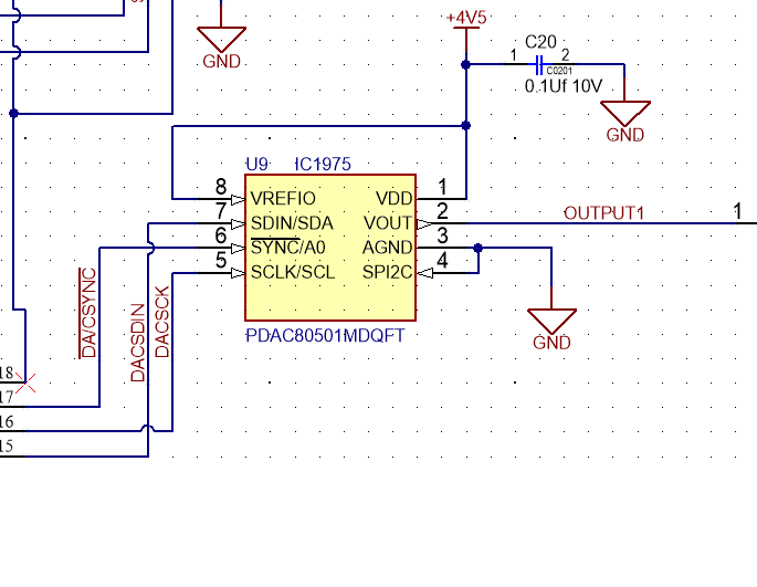
DAC80501: I would like you review the attached implentation of the DAC80501. Note that the VREFIO and VDD are both connected to 4.5V.

$
0
0

Part Number:DAC80501

 I am testing with  DAC05051 EVAL board. I am not used the USB 2any. I am simply connecting 4.5V to VDD and then connecting a jumper to TP8.  With this configuration and noticed that it draws excessive current when 4.5V is connect to Pin 8 VREFIO.  This seems like a problem.  Can you help me with this?


TPL0102EVM: Reading Megaohms Across Rwh

$
0
0

Part Number:TPL0102EVM

We have a National Instruments I2C interface to the TPL0102EVM board. We followed the user guide for setup, but we were unable to get a response from the board. Here are the steps we followed:

  1. Populated R1 and R2 with 4.3Kohm pullup resistors on the SDA and SCL lines
  2. Still had no response, so we tied Vdd to Alt (they were not tied together before). 5V is coming in on Alt line on J14.
  3. Successful response from IC
  4. Sent Binary '0' to I2C address 101 0000‬ (decimal 80 in LabVIEW), A0, A1, A2 = 0
  5. Read ~96K across Rwh
  6. Tried sending various binary data bytes to change Rwh, but could not figure out proper format to send (straight binary, hex, decimal, etc.)
  7. Eventually start reading 2-10 Megaohms, varying wildly across Rwh on both potentiometers

No matter what we send, we are consistently reading Megaohms. Is it possible we blew something? The master is recognizing that the slave received messages just fine. When we send an incorrectly formatted data stream, we get an error which clears when we send a valid data stream. We've tried re-sending the initial '0' stream, but unable to repeat our initial Rwh measurement.

Any thoughts?

ADC08DJ3200: Trying getting erroneous test pattern out of jesd204b

$
0
0

Part Number:ADC08DJ3200

Running the chip at 6.4GHz, 16 Channels of data over JESD204 is working correctly and subclass 0 is running smoothly to a Xilinx MPSoC.  When I run test patterns from the ADC I get bad data on some channels.  Always the same bad channels.

Test pattern 4 or ramp i get errors that are code based.

instead of 0xB0 i get 0xAF

0x64 i get 0x7B

0x67 i get 0x78

Across all 16 channels.  I have not done an exhaustive search in this mapping.

Test pattern 5 or Short Transport Test Pattern 

0x03 => 0x1C

0x05 => 0x1A

0x06 => 0x19

0xFC => 0xE3

0xFA => 0xE5

0xF9 => 0xE6

And in this case it is isolated to 6 of the 16 lanes because of the nature of the test pattern.  This test is the same on both A group of 8 and B group of 8.

Am I not configured correctly?  I have double checked my polarity.

DAC38J84: DAC38J84 spur

$
0
0

Part Number:DAC38J84


Dears.

I have a question about DAC38J84 Spur.

Our condition is as follows

Fs=300Mhz
DACCLK = 2400Mhz
Interpolation = 8

Internal PLL used.

Why does SPUR occur?

Please review.

ADS1291: How to use only the two electrodes of LA and RA of ADS1291 for design?

$
0
0

Part Number:ADS1291

Hi Team,

Customer has a product that uses the ADS1291. There are some questions need your help.
1. There are only two electrodes, LA and RA, and how should the hardware be designed?
2. What are the disadvantages of the solution compared to the three electrodes (RA, LA, RLD)?
3. Without RLD electrodes, common mode interference will be greater, can medical standards be met?

Thanks.

ADS8668: Pull up registor on /CS

$
0
0

Part Number:ADS8668

Hi team,

Is the pull-up registor needed for /CS pin?

Regards,

Saito

Viewing all 5988 articles
Browse latest View live


<script src="https://jsc.adskeeper.com/r/s/rssing.com.1596347.js" async> </script>